April 21-23, 2026
Shanghai

ICPF 2025 to Debut with Upgraded Semiconductor Packaging & Testing Line at NEPCON China

ICPF 2025, held alongside NEPCON China 2025, will make its grand debut from April 22–24 at the Shanghai World Expo Exhibition & Convention Center. The exhibition will introduce an upgraded Demonstration Line for Semiconductor Packaging & Testing Processes, spotlighting advanced process segments such as:

  • Advanced packaging techniques
  • SiC die attach with silver sintering
  • IGBT solder die bonding
  • Wire bonding and testing processes


Advanced Packaging Segment

Flipchip Die Bonder SFM3-FA

Hanwha’s third-generation Flipchip die bonder SFM3-FA has proven mass production performance, validated by global leaders like Samsung and SK Hynix. With top market share in Korea’s flipchip sector, it's widely used in memory production. Key features include:

  • Auto tool exchange (rubber PAD, ejector DOME, COLLET)
  • Flux level detection & refill
  • Die crack detection
  • SECS/GEM E142 protocol for real-time production monitoring
  • UPH up to 10K
  • Die size: 0.5 mm – 46 mm
  • Accuracy: ±5μm @ 3σ


Vertical Curing Oven

MW-OVEN-4035-80 Vertical Curing Oven

This oven uses convection heating to achieve uniform temperature distribution, enhancing material stability post-encapsulation. It supports curing processes for adhesives used in electronic packaging, improving shock resistance, waterproofing, and aging durability.


Full-Automation Jet Ball Placement

HS-M2 Jet Ball Placement Machine

Self-developed to support 2.5D, 3D, and Chiplet packaging, HS-M2 achieves fully automated ball placement, reballing, and unloading. Key highlights:

  • 80–300 balls/second
  • Handles high warpage substrates
  • Tool-less design saves costs and time
  • Ideal for high-mix, low-volume production


SiC Die Attach with Silver Sintering

Online Silver Sintering System – Si 318

Targeting core SiC packaging processes, Quickchip developed this silver sintering system in collaboration with Tsinghua University. Recognized as a first-set major equipment in Jiangsu, it has passed national-level project acceptance and received multiple patents and innovation awards.


High-Density Microwave Plasma Cleaning

AMP-20LA In-Line Plasma Cleaner

Ideal for mass production, the AMP-20LA removes organic contaminants and oxides from material surfaces to improve bonding and welding quality—without physical damage.

Key features:

  • Damage-free cleaning
  • High-density plasma
  • Uniform cleaning across large areas
  • Strong deoxidation capabilities
  • Advanced automation


ND1800 Silver Sintering Die Bonder

Also, from OPTO INTEL, this die bonder ensures high-quality pre-attach for SiC chips, preparing them for reliable silver sintering.

Highlights:

  • Multi-functional platform for IGBT/SiC
  • Supports silver paste or silver film
  • Placement force: 300N (500N optional)
  • Heating up to 200°C
  • UPH 1.8k
  • 360° placement
  • SECS/GEM compatible


Atmospheric Plasma Cleaning

AP-C350 Plasma Cleaner

Focused on green and micro-level cleaning solutions, the AP-C350 uses ionized gases to remove contaminants through chemical reactions—ideal for enhancing product reliability across industries.


Nano-Ag/Nano-Cu Positive Pressure Sintering Furnace

SIN270

Equipped with R&S network analyzers for impedance testing, the SIN270 offers:

  • Real-time waveform storage and report export
  • 0.5 sec/point measurement speed
  • Ethernet communication
  • Custom testing functions
  • MES system integration
  • WIN7/10/11 compatibility


IGBT Solder Die Bonding

IGBT WB/Module AOI System (3D)

Combines 2D/3D modules to inspect for contamination, cracks, chip BLT, wire height, bonding issues, and more. Supports AI algorithms, SECS/GEM protocols, and manual rechecking.


Vacuum Formic Acid Soldering

TFV-300

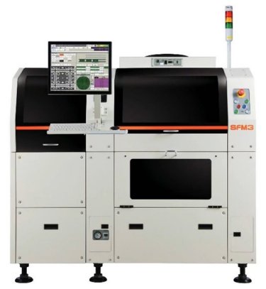
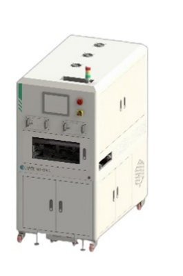
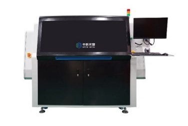
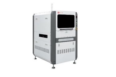
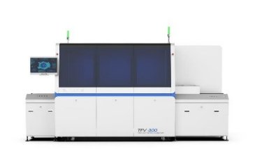
Designed for chip-to-substrate, substrate-to-heatsink, and lid-to-package bonding, this system delivers low-void, high-reliability joints.

Highlights:

  • Supports soldering with paste or preforms
  • Heating up to 400°C
  • Chamber pressure ≤1mbar
  • <1% void rate
  • Supports N₂, H₂, and formic acid atmospheres


Join us at NEPCON China 2025 April 22-24, 2025, for an unparalleled opportunity to expand your network, engage in direct business matchmaking, and access innovative technologies that will shape the future of electronics manufacturing!

Pre-register for NEPCON China 2025: https://ali2.infosalons.com.cn/reg/NEPCON25SH/registeren/login?type=WE9ZIC

If interested in exhibiting at NEPCON China, please contact

Ms. Julia Gu

Tel: +86 21-2231-7010

Email: [email protected] 


If interested in visiting NEPCON China, please contact

Mr. Walden Li

Email:  [email protected], [email protected]  

Mobile/WhatsApp/WeChat:  +86 136-5125-1335


For TAP service, please contact:

Mr. Alan Li

Email: [email protected]


For media partnerships, please contact:

Ms. Yuri Yu 

E-mail: [email protected][email protected]  


Ms. Chopin Mo 

E-mail: [email protected]


Follow us on:

Facebook: @NEPCONASIA

Twitter: @Nepcon_Official

LinkedIn: @NEPCON ASIA